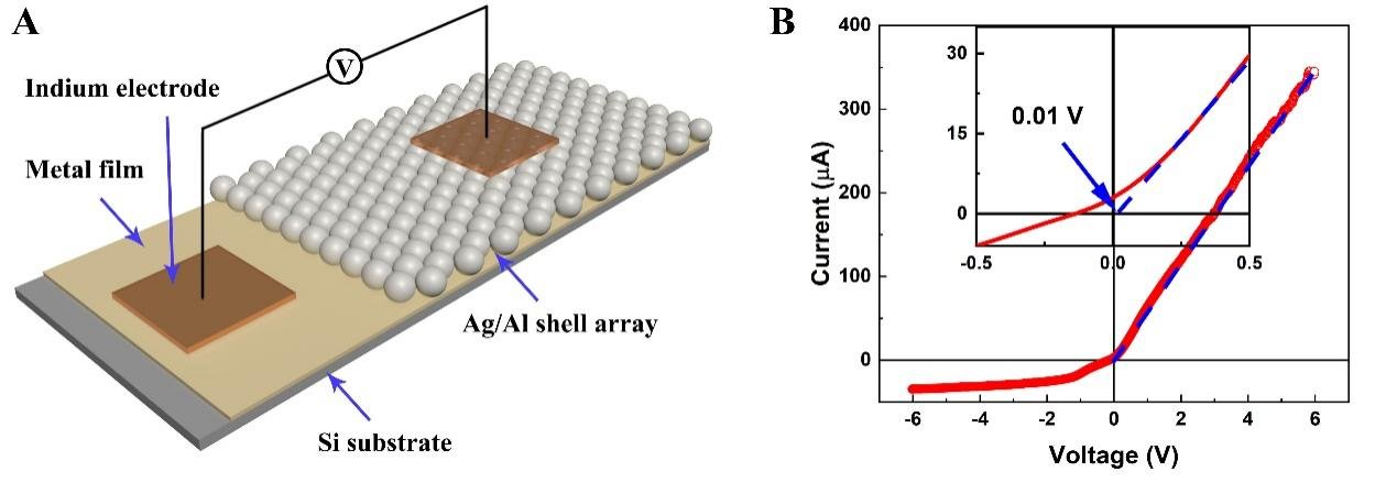

Ag/Al shell array
(A) A schematic diagram of p-n junction structure and testing (partial enlarged view)
(B) I-V curve at room temperature

Prof. Li Zhigang (middle), undergraduates Li Jiteng (right) and Zhou Youngrui (left)
Recently, under the guidance of Prof. Li Zhigang, two undergraduates from the School of Materials Science and Engineering, Class of 2020, majoring in material physics, Li Jiteng and Zhou Yongrui, have for the first time in the world synthesized p-n junctions with semiconductor properties based on metal nanoarrays. Their research paper, titled Near Zero-threshold Voltage P-N Junction Diodes Based on Super-semiconducting Nanostructured Ag/Al Arrays, with Taizhou University as the first author affiliation, was published in the international authoritative journal Advanced Materials (IF: 32.086).
Semiconductor devices are one of the most common energy-consuming devices in everyday life. Power consumption is one of the key bottlenecks limiting the performance improvement of semiconductor chips. Compared with conventional semiconductors, metals usually consume less power at the same current. However, it is more difficult to produce functional devices based entirely on metals, such as p-n junction diodes, transistors and chips because of the large number of free electrons in metals. In recent years, Prof. Li Zhigang’s team, in close collaboration with Prof. Wei Bingqing from the University of Delaware, have discovered for the first time that metallic bi-layer shell arrays exhibit semiconductor transport behavior with ultra-low resistivity and successfully constructed p-n junction diodes with pure metal nanoarrays. The team constructed the Ag/Al bimetallic shell structure (where Ag is the plasmon resonance layer and Al is the electron transport layer) by magnetron sputtering through colloidal crystal template etching. At the same time, an Ag film is deposited on the substrate to prevent the formation of Schottky contacts between the shell array and the silicon substrate. Compared with the conventional semiconductor p-n junction, the metal plasmon resonance-based p-n junction has two major advantages: ① Ultra-low power consumption. The achievement of near zero-threshold voltage in p-n junction diodes based on super-semiconducting nanostructured Ag/Al arrays is reported, realizing ultra-low-power p-n junction diodes: ≈3 W per trillion diodes with a working voltage of 1 V or 30 mW per trillion diodes with an operating voltage of 0.1 V. ② High breakdown field. Due to a robust built-in field driven by infrared light photons, the p-n junction diodes exhibit a high breakdown field of ≈1.1 × 10⁶ V cm−1, similar to that of SiC and GaN. (links for more information: https://onlinelibrary.wiley.com/doi/10.1002/adma.202210612)
Attaching great importance to the improvement of students’ scientific research ability, Taizhou University encourages students to closely integrate into faculty research teams and produce scientific research results. According to statistics, a total of 6 papers were published by students from School of Materials Science and Engineering as the first authors or co-authors on SCI Q1 and other top journals in 2022.